
Join our discord server and subreddit for more intellect discussions.
Follow our blog “Big Brains”, if you like the content we post.
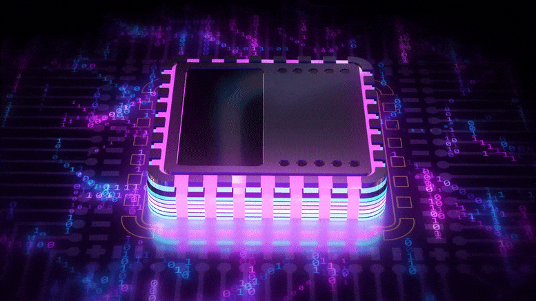
Year after year, the explosive growth of computing power relies on manufacturers’ ability to suit more and more components into an equivalent amount of space on a chip . That progress, however, is now approaching the bounds of the laws of physics, and new materials are being explored as potential replacements for the silicon semiconductors long at the guts of the pc industry.
New materials can also enable entirely new paradigms for individual chip components and their overall design. One long-promised advance is that the ferroelectric FET , or FE-FET. Such devices could switch states rapidly enough to perform computation, but even be ready to hold those states without being powered, enabling them to function as LTM storage. Serving double duty as both RAM and ROM, FE-FET devices would make chips more room efficient and powerful.
The hurdle for creating practical FE-FET devices has always been in manufacturing; the materials that best exhibit the required ferroelectric effect aren’t compatible with techniques for mass-producing silicon components due the heat requirements of the ferroelectric materials.


Now a team of researchers at the University of Pennsylvania School of Engineering and engineering has shown a possible way around this problem. during a pair of recent studies, they need demonstrated that scandium-doped aluminum nitride (AlScN), a cloth recently discovered to exhibit ferroelectricity, are often wont to make FE-FET also as diode-memristor-type memory devices with commercially viable properties.
The studies were led by Deep Jariwala, professor in Electrical and Systems Engineering (ESE), and Xiwen Liu, a grad student in his lab. They collaborated with fellow Penn Engineering faculty members Troy Olsson, also an professor in ESE, and Eric Stach, professor within the Department of Materials Science and Engineering and Director of the Laboratory for Research on the Structure of Matter.
They published their findings within the journals Nano Letters and Applied Physics Letters.
“One of the most ways in which chip designers are brooding about getting round the looming limitations of processing vast amounts of knowledge with silicon is finding materials that might allow memory components to be built directly on top of the processor without harming the processor within the process, essentially making two-in-one devices,” says Jariwala. “Since AlScN are often deposited at relatively low temperatures, we knew it represented an opportunity for directly combining memory with logic transistors. We just needed how to integrate it with the remainder of the chip architecture.”
Jariwala and his colleagues found an answer during a promising two-dimensional material referred to as molybdenum disulfide, or MoS2. employing a single layer of MoS2 as a channel out of an AlScN-based FE-FET device, the team was ready to test its switching speed and memory stability. Those results were published in their Nano Letters paper.
“Engineers are pursuing the concept of FE-FET memory since the 60s, since these devices could operate at extremely low powers,” says Jariwala. “The issue really has been to form their fabrication compatible with processors and make them last longer. this is often where our 2D materials come in; they’re so thin that when a memory bit is written in them, they might preserve that information within the sort of charge for years.”
Jariwala and his colleagues’ next steps were to shrink the size of their memory devices. In their Applied Physics Letters paper, they demonstrated the power to supply AlScN as thin as 20 nanometers, reducing the general size of the device also because the voltage it requires.
“Prior to the present study, it wasn’t clear that AlScN would retain the required ferroelectric properties while cutting down to the present size,” says Olsson.
“We also found that removing the MoS2 and using AlScN during a two-terminal device geometry allows it to function as a diode-memristor-like storage device ,” adds Stach. “Diode memristors are simpler than FE-FET devices and even easier to integrate on a billboard scale since they require fewer steps and components.
Jariwala and his colleagues will still investigate manufacturing techniques for these devices that might allow them to be mass-produced and integrated into consumer electronics.
References:
“Post-CMOS Compatible Aluminum Scandium Nitride/2D Channel Ferroelectric Field-Effect-Transistor Memory” by Xiwen Liu, Dixiong Wang, Kwan-Ho Kim, Keshava Katti, Jeffrey Zheng, Pariasadat Musavigharavi, Jinshui Miao, Eric A. Stach, Roy H. Olsson III and Deep Jariwala, 21 April 2021, Nano Letters.
DOI: 10.1021/acs.nanolett.0c05051
“Aluminum scandium nitride-based metal–ferroelectric–metal diode memory devices with high on/off ratios” by Xiwen Liu, Jeffrey Zheng, Dixiong Wang, Pariasadat Musavigharavi, Eric A. Stach, Roy Olsson III and Deep Jariwala, 18 May 2021, Applied Physics Letters.
DOI: 10.1063/5.0051940
Former postdoctoral researchers Dixiong Wang and Jinshui Miao, graduate students Kwan-Ho Kim and Jeffrey Zheng, undergraduate Keshava Katti, and current postdoctoral researcher Pariasadat Musavigharavi, all of Penn Engineering, also contributed to the research.
The research was supported by the Defense Advanced Research Projects Agency (DARPA) TUFEN program under Agreement No. HR00112090046, and therefore the Penn Center for Undergraduate Research and Fellowships. The work was administered partially at the Singh Center for Nanotechnology at the University of Pennsylvania, which is supported by the National Science Foundation (NSF) National Nanotechnology Coordinated Infrastructure Program through grant NNCI-1542153. Facilities and instrumentation utilized in the research are supported by the NSF through the University of Pennsylvania Materials Research Science and Engineering Center (MRSEC) grant DMR-1720530. Sample preparation was performed at the middle for Functional Nanomaterials, Brookhaven National Laboratory, which may be a U.S. Department of Energy (DOE) Office of Science Facility, at Brookhaven National Laboratory under Contract No. DE-SC0012704.